VCXO circuit


The basic RF circuit design for an VCXO comprises a standard crystal oscillator but with an electronic means of tuning or "pulling" the frequency slightly.
This adjustment of the frequency is almost invariably achieved using varactor or varicap diodes. In most VCXOs a pair of back to back diodes are placed across the crystal.
A reverse bias is applied to anodes of the diodes which then act as a variable capacitor across the crystal. In most cases a Colpitts oscillator circuit is used as this provides a reliable RF design for this type of oscillator.
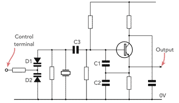
Typical VCXO circuit
The amount by which the crystal frequency can be pulled depends upon a variety of factors including the level of capacitance applied, the circuit conditions themselves and the crystal.
However the frequency cannot be pulled too far, because the activity of the crystal reduces as the level of capacitance across the crystal increases. This wil reduce the output and overall performance.
If it is necessary for the VCXO to be pulled over a large range, then an inductor can be incorporated into the circuit. Again, care is needed with the RF design to ensure the performance does not fall too far.
If too much inductance is added, then the circuit can become unstable and spurious signals may be generated, of the frequency of oscillation may not be controlled by the crystal. Any commercially manufactured oscillator will have been fully tested to ensure its reliable operation.